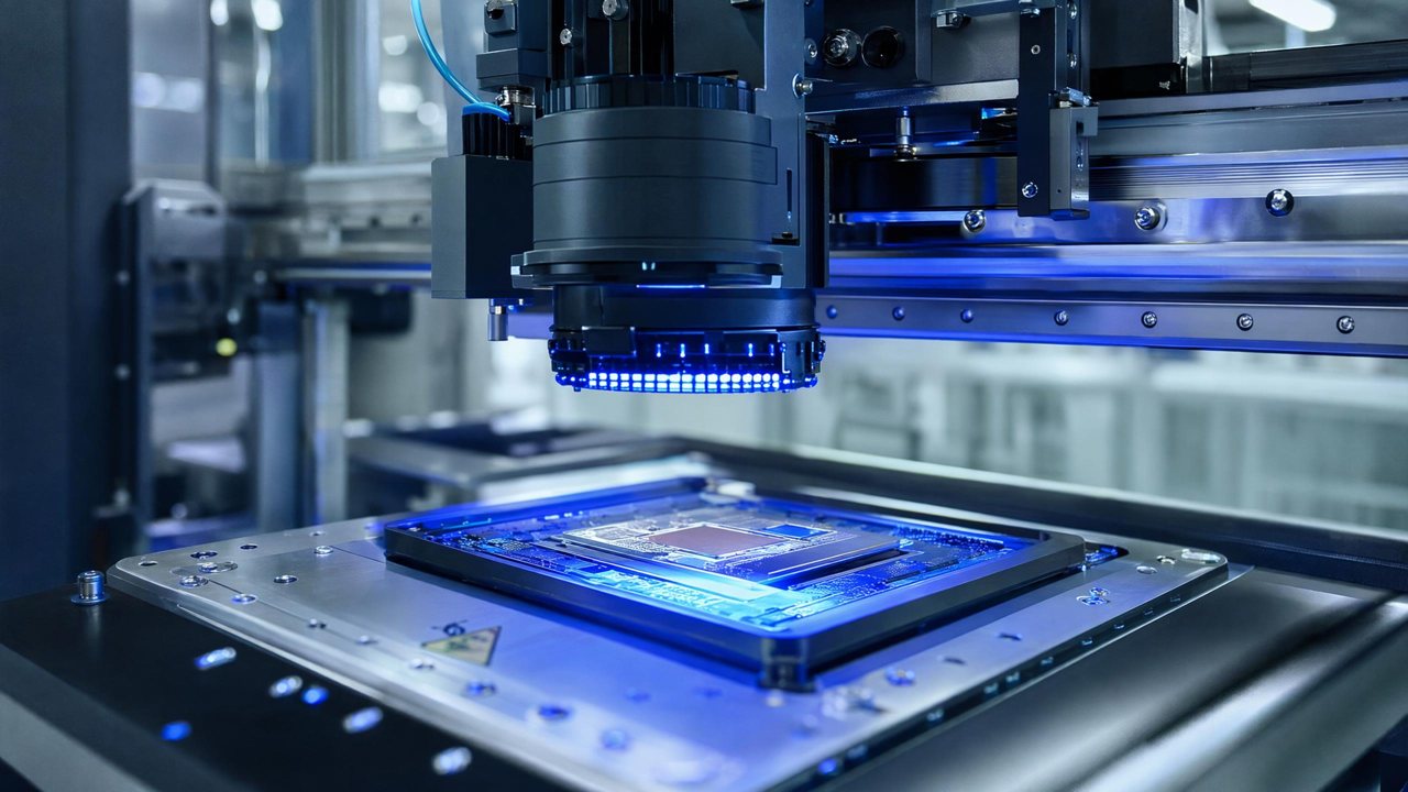
In the semiconductor chip production process, the quality inspection of micro-bumps is a crucial step to ensure the performance and reliability of chips. WeLinkirt's 3D AI AOI equipment brings new breakthroughs in solving the problem of micro-bump defect detection.
In the era of rapid technological development today, the semiconductor industry, as the core of modern electronic technology, directly affects the trend of the global technology industry. Semiconductor chips are widely used in many fields such as smartphones, computers, and automotive electronics, which puts forward extremely high requirements for their performance and reliability. In the semiconductor chip production process, chip packaging is a crucial step. It can not only protect the chip but also realize the electrical connection between the chip and the outside world. As the key connection between the chip and the packaging substrate, the quality of micro-bumps directly determines the performance and reliability of the chip. A leading semiconductor manufacturer deeply realizes the importance of accurate quality inspection of micro-bumps in the micro-bump welding process of its chip packaging production line. Any defects in micro-bumps, such as missing or bridging, may cause performance failures of the chip, affecting the overall quality and market competitiveness of the product. Therefore, efficient and accurate quality inspection of micro-bumps has become an urgent problem for the manufacturer to solve.
Pain Points: Why It's Difficult
Traditional detection methods face many difficulties in micro-bump defect detection. Firstly, a high false-negative rate is a prominent problem. Under the traditional detection mode, about 3% of micro-bump defects cannot be detected. This is because the accuracy of traditional detection equipment is limited, and it is difficult to accurately identify some tiny defects, such as micron-level pores and slight bridging. These undetected defective chips flowing into subsequent processes will not only increase the production risk but also lead to a significant increase in production costs. Once problems are found in subsequent processes, rework or scrapping is required, wasting a large amount of manpower, material resources, and time.
Secondly, a high false-positive rate is also a major drawback of traditional detection methods. The false-positive rate of traditional detection equipment reaches 15%, and a large number of false-positive information brings great trouble to production. This is due to the limitations of traditional detection algorithms, which are difficult to accurately distinguish between normal micro-bumps, normal situations with slight differences, and real defects. A large number of false-positives require manual re-inspection, which not only wastes a lot of labor costs but also seriously reduces the production efficiency of the production line, making the entire production process cumbersome and inefficient.
In addition, the long change-over time of traditional detection equipment is also a problem that seriously affects the production flexibility. Each change-over takes 30 minutes because the adjustment and calibration process of traditional equipment is relatively complex, requiring a large amount of manual parameter setting and debugging. In today's market with rapidly changing demands, the long change-over time makes it difficult for the production line to quickly respond to the production needs of different products, reducing the market competitiveness of the enterprise.
Technical Principle
WeLinkirt's 3D AI AOI equipment uses a self-developed 3D camera for image acquisition, and its working principle is based on the structured light three-dimensional measurement technology. This technology projects a specific structured light pattern onto the measured object and then uses the camera to capture the deformation of the pattern reflected from the object surface. Since defects such as missing or bridging of micro-bumps will cause changes in the surface topography, this change will be directly reflected in the reflected pattern. The equipment uses a three-dimensional topography reconstruction algorithm to convert the collected deformed pattern data into three-dimensional point cloud data, thus accurately restoring the real three-dimensional topography of micro-bumps. Compared with traditional 2D detection methods, 3D point cloud data can provide more comprehensive information and has stronger detection ability for defects in 2D optical blind areas such as hidden solder joints, coplanarity, and micron-level topography.
The equipment also uses 2D-3D fusion technology, which combines the texture information of 2D images with the topography information of 3D point clouds. This fusion technology further improves the accuracy and reliability of defect detection. 2D images can provide the texture details of the micro-bump surface, while 3D point clouds can reflect its real three-dimensional shape. The combination of the two can analyze the features of micro-bumps more comprehensively, thus more accurately identifying various defects. In terms of algorithms, the equipment uses an advanced deep-learning algorithm to train a large number of micro-bump samples. Through this training, the model can automatically learn the normal and defect features of micro-bumps, thus realizing the accurate classification and identification of micro-bump defects. Compared with traditional rule-based algorithms, deep-learning algorithms have stronger adaptability and self-learning ability and can better handle complex and changeable micro-bump defect situations.
Typical Application Scenarios
- Missing micro-bump detection: In the micro-bump welding process of the chip packaging production line, missing micro-bumps are a common defect. The 3D AI AOI equipment accurately measures the three-dimensional topography of micro-bumps and compares it with the three-dimensional model of normal micro-bumps. If the height of a micro-bump at a certain position is significantly lower than the normal range or no corresponding three-dimensional point cloud data is detected, it can be judged that the micro-bump is missing. The difficulty lies in the tiny size of micro-bumps, which requires the equipment to have extremely high accuracy and resolution.
- Micro - bump bridging detection: Micro - bump bridging refers to the abnormal connection between adjacent micro-bumps, which will cause problems such as circuit short-circuits. The equipment uses 2D-3D fusion technology, combining the texture information of 2D images and the topography information of 3D point clouds. If there are abnormal connection traces between adjacent micro-bumps in the 2D image and the topography of this area in the 3D point cloud does not meet the normal situation, it can be accurately judged as a bridging defect. The difficulty lies in that the bridging part may be very subtle, and the equipment needs to be able to accurately capture these subtle changes.
- Hidden solder joint detection: Hidden solder joints refer to the solder joints that are blocked by other components or inside the chip, and traditional 2D detection methods are difficult to detect them. The 3D point cloud data of the 3D AI AOI equipment can penetrate a certain degree of occlusion and obtain the three-dimensional topography information of hidden solder joints. By analyzing this information, it can be judged whether there are defects such as false soldering or missing soldering in hidden solder joints. The difficulty lies in the weak signal of hidden solder joints, which requires the equipment to have strong signal processing and analysis capabilities.
- Coplanarity detection: The coplanarity of micro-bumps is crucial for the electrical connection and performance of the chip. The equipment analyzes the three-dimensional point cloud data of micro-bumps and calculates the height difference of each micro-bump. If the height difference exceeds the specified range, it means that the coplanarity of micro-bumps does not meet the requirements. The difficulty lies in the need to accurately measure and calculate a large number of micro-bumps to ensure the accuracy of the detection results.
- Micron - level topography detection: Micron - level topography defects on the surface of micro-bumps, such as tiny protrusions and depressions, will also affect the performance of the chip. The equipment uses a high-precision 3D camera and an advanced three-dimensional topography reconstruction algorithm to detect these micron-level topography changes. The difficulty lies in the need for the equipment to have extremely high accuracy and sensitivity to capture these tiny changes.
Implementation Case
A leading semiconductor manufacturer occupies an important position in the global semiconductor market. Its production scale is large, and its chip packaging production line is busy. The manufacturer has always been committed to improving product quality and production efficiency. After facing many problems caused by traditional detection methods, it decided to introduce WeLinkirt's 3D AI AOI equipment. During the equipment installation process, WeLinkirt's technical team closely cooperated with the manufacturer's engineers to conduct detailed installation, debugging, and training of the equipment. After a period of trial operation and optimization, the equipment was successfully put into formal use.
WeLinkirt's 3D AI AOI equipment has brought a qualitative leap to semiconductor chip micro-bump detection, significantly improving detection efficiency and accuracy.
WeLinkirt's Solution and Products
Centered on the 3D AI AOI equipment, WeLinkirt provides a complete defect detection solution for the semiconductor manufacturer. The equipment can detect various defects of micro-bumps with high accuracy by virtue of the self-developed 3D camera and advanced three-dimensional topography reconstruction technology. The supporting DaoAI AI AOI software system has a strong feature recognition ability of the visual basic model. With only one good sample, 0-code automatic programming can be completed in 5 minutes, greatly shortening the programming time. Through APDT positive-sample/few-sample learning (only 1-20 good samples are needed) and combined with the semantic false-positive filtering function, the false-positive situation is effectively reduced. This software-hardware combined solution provides an efficient and accurate means for semiconductor manufacturers to detect micro-bump defects.
Quantitative results: After using WeLinkirt's 3D AI AOI equipment, the defect detection rate of the manufacturer has increased significantly to 99.2%, and the false-negative rate has decreased to <0.8%. The false-positive rate has decreased by -68%, greatly reducing the manpower and time costs for re-inspection. At the same time, the equipment change-over time has been shortened to 5 minutes, improving the flexibility and production efficiency of the production line. These significant quantitative results fully prove the excellent performance of WeLinkirt's 3D AI AOI equipment in the field of semiconductor micro-bump detection.
FAQ
What types of micro-bump defects can the 3D AI AOI equipment detect?
The 3D AI AOI equipment can detect common micro-bump defects such as missing and bridging, as well as defects in 2D optical blind areas such as hidden solder joints, coplanarity, micron-level topography, and pores. It uses 2D-3D fusion technology to combine the texture of 2D images with the topography information of 3D point clouds, improving the detection accuracy.
How much can the change-over time be shortened after using this equipment?
After using the 3D AI AOI equipment, the change-over time can be shortened from the traditional 30 minutes to 5 minutes. This greatly improves the flexibility of the production line, enabling it to respond more quickly to the production needs of different products and enhancing the market competitiveness of the enterprise.
What role does the supporting software system play in reducing false-positives?
The supporting DaoAI AI AOI software system has the feature recognition ability of the visual basic model. Through APDT positive-sample/few-sample learning (only 1-20 good samples are needed) and combined with the semantic false-positive filtering function, it can effectively identify normal micro-bumps and defects, reduce false-positives, and lower the manpower and time costs for re-inspection.
This article was generated by AI. Customer cases are simulated scenarios based on real product capabilities and figures are illustrative; see product pages for official benchmarks.