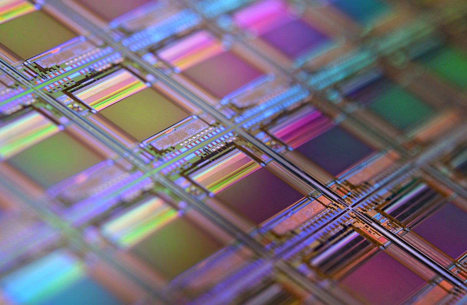
The development of the semiconductor industry has increasingly strict requirements for wafer quality, and traditional inspection methods are no longer able to meet the needs. WeLinkirt uses AI vision technology to bring new breakthroughs to semiconductor wafer map defect inspection.
In the semiconductor industry, wafers are the core carriers for chip manufacturing, and their quality directly determines the performance and reliability of chips. In the wafer manufacturing line of a leading semiconductor manufacturer, the production of wafers is a highly complex and precise process. From the growth and slicing of silicon ingots to a series of processes such as photolithography, etching, and doping on the wafer surface, each step may introduce various microscopic defects. These defects may exist on the surface, inside the wafer, or in the structure of the microscopic patterns. Therefore, high-precision detection of various defects on the wafer map is a crucial step to ensure that the quality and performance of the wafer meet the standards. Only through strict inspection can qualified wafers be selected for the subsequent chip manufacturing process, thus ensuring the quality and stability of the final product.
Pain Points: Why Is It Difficult?
Traditional inspection methods face many quantitative difficulties. First of all, the miss-detection rate is relatively high, about 3%. This means that some defective wafers may flow into the subsequent processes, bringing serious hidden dangers to the entire production process. Once these defective wafers enter the chip manufacturing stage, it may lead to unstable chip performance and a decrease in the yield rate, thereby increasing production costs. Secondly, the false-alarm rate reaches 20%. Frequent false alarms will make operators spend a lot of time verifying and processing false alerts, which not only increases labor costs but also reduces production efficiency. For example, in a busy production line, each false alarm may interrupt the normal production rhythm and cause production delays. In addition, the change-over time is relatively long, requiring 30 minutes for each change-over. In semiconductor production, different types of wafers may require different detection parameters and processes. A long change-over time will seriously affect the flexibility and production rhythm of the production line, making it difficult for the production line to quickly respond to changes in market demand.
The root cause of these problems lies in the limitations of traditional inspection methods. Traditional methods often rely on fixed rules and templates for defect identification, making it difficult to adapt to complex and changeable wafer defect patterns. Moreover, traditional 2D inspection methods can only obtain the planar information of the wafer surface, and are prone to miss-detect defects hidden inside the wafer or with complex three-dimensional structures. At the same time, due to the lack of intelligent learning and self-adaptation capabilities, traditional methods cannot adjust the detection strategy in time when facing new defect types or process changes, resulting in a high false-alarm rate.
Technical Principle
WeLinkirt uses advanced deep-learning algorithms and high-precision imaging technology. The deep-learning algorithm is trained with a large number of wafer map samples and can learn the characteristics and laws of different defect patterns. During the training process, the algorithm will conduct a detailed analysis of each sample and extract the key features of defects, such as shape, size, color, and texture. Through continuous learning and optimization, the algorithm can establish an accurate defect classification model, thereby accurately identifying various tiny defects. Compared with traditional rule-based methods, deep-learning algorithms have powerful feature extraction and classification capabilities, can automatically adapt to different types of wafers and defect patterns, and greatly improve the accuracy and stability of detection.
In terms of imaging, WeLinkirt uses its self-developed 3D camera for data collection and combines three-dimensional topography reconstruction technology to obtain detailed three-dimensional information of the wafer surface. The 3D camera can photograph the wafer from different angles to obtain rich image data. Then, through the three-dimensional topography reconstruction technology, these image data are converted into an accurate three-dimensional model, which can clearly show the microscopic structure and defect situation of the wafer surface. This method avoids the possible miss-detection problems of traditional 2D inspection methods because it can detect defects hidden under the surface or with complex three-dimensional structures. For example, for some tiny holes, protrusions, or internal impurities, the 3D detection method can identify and locate them more accurately.
Typical Application Scenarios
- Photolithography process inspection: In the photolithography process, there may be defects such as deformation, missing, or misalignment of the photolithography pattern. WeLinkirt's system uses deep-learning algorithms to accurately analyze the photolithography pattern and identify the characteristic differences between normal and defective patterns. The difficulty lies in the fact that the photolithography patterns are very tiny, requiring extremely high precision. Traditional methods are difficult to accurately detect tiny deformations and misalignments.
- Etching process inspection: The etching process may cause problems such as uneven etching, over-etching, or under-etching on the wafer surface. The 3D camera can obtain the three-dimensional topography information of the wafer surface, and analyze the flatness and depth of the etched surface through three-dimensional topography reconstruction technology. The difficulty lies in the complex microscopic structure of the etched surface. Traditional 2D inspection methods cannot accurately judge the quality of etching.
- Doping process inspection: There may be uneven impurity distribution or non-compliant doping concentration during the doping process. The system can analyze the element distribution on the wafer surface and detect the distribution and concentration of impurities using high-precision imaging technology. The difficulty lies in the extremely small content of impurities, and the detection requires highly sensitive equipment and algorithms.
- Surface scratch inspection: There may be various scratches on the wafer surface, which may affect the electrical performance of the wafer. The deep-learning algorithm can identify the shape, length, and depth of scratches and accurately judge whether the scratches will affect the wafer. The difficulty lies in the diverse forms of scratches, and some scratches are very subtle, easy to be missed.
Implementation Case
A large semiconductor manufacturer has a large-scale wafer manufacturing line and needs to process a large number of wafers every day. Before introducing WeLinkirt's solution, the manufacturer had been facing problems such as low inspection efficiency, high false-alarm rate, and long change-over time. During the implementation process, WeLinkirt's team integrated the DaoAI 2D / 3D AI AOI equipment with the production line, deployed it through SDK / API / Docker, and supported 100% local privatization to ensure that the data did not leave the factory. At the same time, professional training was provided to the operators to enable them to use the DaoAI AI AOI software system proficiently.
WeLinkirt's solution brings a new, efficient, and accurate option for semiconductor wafer map defect inspection.
Before the implementation, the defect detection rate of the manufacturer's wafer map was about 97%, the miss-detection rate was 3%, the false-alarm rate was 20%, and the change-over time was 30 minutes. After the implementation, the detection rate remained above 97%, the miss-detection rate was reduced to <3%, the false-alarm rate was reduced by -60%, greatly reducing labor costs and re-inspection workload. The change-over time was shortened to 5 minutes, and the flexibility and production rhythm of the production line were significantly improved.
WeLinkirt's Solution and Products
The DaoAI AI AOI software system and DaoAI 2D / 3D AI AOI equipment provided by WeLinkirt are the keys to solving this problem. The DaoAI AI AOI software system has the feature recognition ability of a visual basic model. Only 1-20 good wafers are needed, and zero-code automatic programming can be realized within 5 minutes. This means that operators do not need to have professional programming knowledge to quickly set detection parameters and rules. At the same time, the software system uses APDT positive-sample/few-sample learning and semantic false-alarm filtering technology to effectively reduce false alarms. Through learning from positive samples, the system can accurately identify normal wafer patterns and better judge the existence of defects. The semantic false-alarm filtering technology can intelligently analyze and filter false-alarm information, only retaining real defect alerts.
The DaoAI 2D / 3D AI AOI equipment combines the self-developed 3D camera and three-dimensional topography reconstruction technology. The 3D camera can obtain the three-dimensional information of the wafer surface, detect hidden solder joints, coplanarity, and micron-level topography, improving the accuracy and comprehensiveness of detection. The equipment can accurately analyze the microscopic structure of the wafer surface and timely discover various potential defects. In practical applications, the equipment can be smoothly integrated with the production line to realize an automated inspection process and improve production efficiency.
Quantitative Results
By using WeLinkirt's solution, the defect detection rate of the semiconductor manufacturer's wafer map has been increased to over 97%, and the miss-detection rate has been reduced to <3%. The false-alarm rate has been reduced by -60%, greatly reducing labor costs and re-inspection workload. The change-over time has been shortened to 5 minutes, and the flexibility and production rhythm of the production line have been significantly improved. These quantitative results show that WeLinkirt's solution can effectively solve the problem of semiconductor wafer map defect detection and bring significant economic benefits and production efficiency improvements to the enterprise.
FAQ
How does WeLinkirt solve the problem of semiconductor wafer map defect inspection?
WeLinkirt uses advanced deep-learning algorithms and high-precision imaging technology. The algorithm is trained with a large number of samples to learn defect features. At the same time, the self-developed 3D camera and three-dimensional topography reconstruction technology are used to obtain the three-dimensional information of the wafer. It also provides the DaoAI AI AOI software system and DaoAI 2D / 3D AI AOI equipment to improve detection accuracy, reduce false alarms, and shorten the change-over time.
What quantitative results can WeLinkirt's solution bring?
By using WeLinkirt's solution, the defect detection rate of semiconductor manufacturers' wafer maps can be increased to over 97%, the miss-detection rate can be reduced to <3%, the false-alarm rate can be reduced by 60%, and the change-over time can be shortened to 5 minutes. This significantly improves the flexibility and production rhythm of the production line and reduces labor costs and re-inspection workload.
What are the advantages of WeLinkirt's DaoAI AI AOI software system?
The software system has the feature recognition ability of a visual basic model. Only 1-20 good wafers are needed, and zero-code automatic programming can be realized within 5 minutes. It uses positive-sample/few-sample learning and semantic false-alarm filtering technology to effectively reduce false alarms, allowing operators to quickly set detection rules.
This article was generated by AI. Customer cases are simulated scenarios based on real product capabilities and figures are illustrative; see product pages for official benchmarks.